North Bridge, GIO and Memory Controller
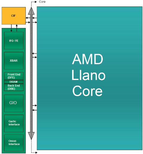
In the figure is shown a simplified block diagram of the architecture of the heart of Llano, ie components that track data and manage communication with the outside world: the North Bridge, the GIO unit and the memory controller.

The green block, containing the elements called IFQ/FE, Xbar, Front End (DFE), DRAM, Back End (DBE), GIO, Garlic Interface and Onion Interface, are on the chip north bridge, abbreviated to CNB.
The yellow block, called CIF is a block of synchronization between the CNB and each core, which unifies and directs the flow of data to and from the cores with the CNB. Its task is to implement the CCI interface, Common Core Interface, which is the single point of access to CNB for all cores.
This block is one that implements the algorithm that decides which of the core can speak in a given time and sorts requests from other parts of the chip to the core, such as cache probing, which is performed to see if the core cache has newer data than the RAM.
Now for the building blocks of the CNB.
The IFQ/FE block contains the request queue of the CPU and GPU in the IFQ that is thus an unified queue.
It also includes a logic block, called the Front End (FE) that handles requests for data transfer to and from the cores (which go through the CCI interface), to manage requests to transfer data between the Onion interface and CPU, to handle requests for CPU cache probing by the various components and to maintain the coherence and consistency between the various units.
Xbar block is the so-called crossbar switch, ie the unit that allows the connection between the various units connected to the CNB.
It's basically a digital switch that connects every moment sender and receiver of a communication between the various actors in the system, such as the CCI interface, the controller RAM, Onion and Garlic interfaces, and so on.
DRAM blocks, DBE and DFE are part of the memory controller (MC).
The DFE block, called data front-end, select the requests to send to the rest of the RAM controller and decides between Onion (coherent) , Garlic (not coherent) and CCI (coherent) requests.
Requests are physically carried out by the DBE block, called Data Back End, which synchronizes the CNB with the physical interface to DRAM and sends transfer commands to it.
Garlic interface is a bi-directional, low latency connection, and so it's direct, between the GPU and RAM controller Data Back-end.
When the Data Front End has given the consent, the GPUs can communicate with the controller RAM directly.
Onion interface is a bidirectional connection between the GPU and the IFQ queue. It's used to connect the CPU to the GPU.

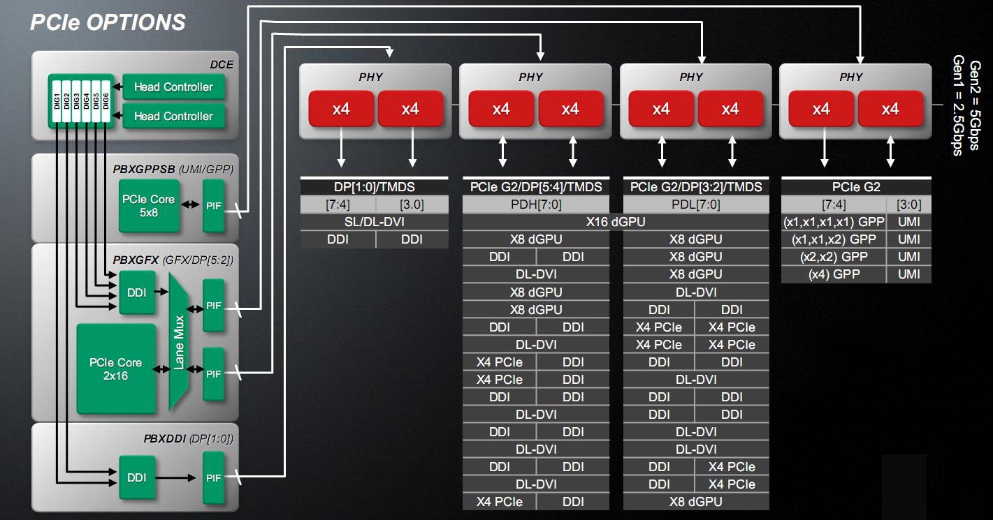
The block indicated with GIO (Graphics and I/O) is the block that handles the chip I/O, and is connected to the Xbar unit of the North Bridge (CNB) to communicate with the core and the RAM controller and has a direct and privileged link with the GPU. This is because the controller manages up to 32 PCI Express lines, configurable in many ways.
Four lines are reserved for the UMI interface (Unified Media Interface), which is nothing more than a 4 lines PCI Express link dedicated to the connection with the Fusion Controller Hub (FCH, the south bridge).
Four PCI Express are reserved for various devices, such as sound cards, to not having to impair the FCH and configurable as single lines, double lines, two singles and a double line or a single x4 interface.
Sixteen lines are used for discrete graphics cards, configured in a x16 interface or two x8 interfaces, for CrossFire.
Alternatively, interfaces can be configured as x8 video outputs, in order to use the Eyefinity technology, losing the possibility of CrossFire/DualGraphics.
The remaining 8 lines are used to implement HDMI, DVI and Display Port interfaces.
The gray BUS that you see on the side of the CNB and the CIF is the only bus connection onto which all the core are connected and on which they are enabled to communicate, in turn, from the CIF block.
Integrated RAM Controller
The Llano RAM controller supports dual independent 64-bit channel of DDR3 RAM with 8-bit and 16 bit chip, supporting chip and channel interleaving useful to increase performance by reading consecutive data from several chips in parallel, includes scheduling algorithms for the opening and closing of memory pages, especially optimized for interspersed read and write streams, includes scheduling algorithms to optimize the interspersed data flow from the CPU+Onion and Garlic interfaces and includes an hardware prefetcher.
In particular, the pages used by the GPU accesses are closed immediately, because they generally are streaming accesses, to free pages for CPU accesses, typically more varied.
The data loaded by the prefetcher are maintained in the controller itself and not speculatively sent to L1 and L2 caches.
The prefetcher is able to capture both increasing or decreasing access trends even with non-uniform spacing, using as measure unit the cache line (64 bytes) and is able to detect even separate sequences of accesses. Llano also can keep track of 8 sequences of accesses simultaneously (Stars architecture can keep track of 5 of it).
The Llano memory controller has been greatly improved compared to the Stars cores. It was improved internal efficiency and prefetching algorithms, in particular the Llano core is able to better recognize patterns of memory access, because it is able to associate the actual instruction that accesses memory (IP-based prefetching) and thus is no longer distracted by other instructions in between. In addition, internal buffers have been increased.
The supported RAM frequency was increased up to 1866 MHz (with one DIMM per channel only), compared to the 1333 MHz of the previous generation. On the other hand DDR2 memory, 4-bit chip and ECC correction support was removed, the latter typically used on the server side.


